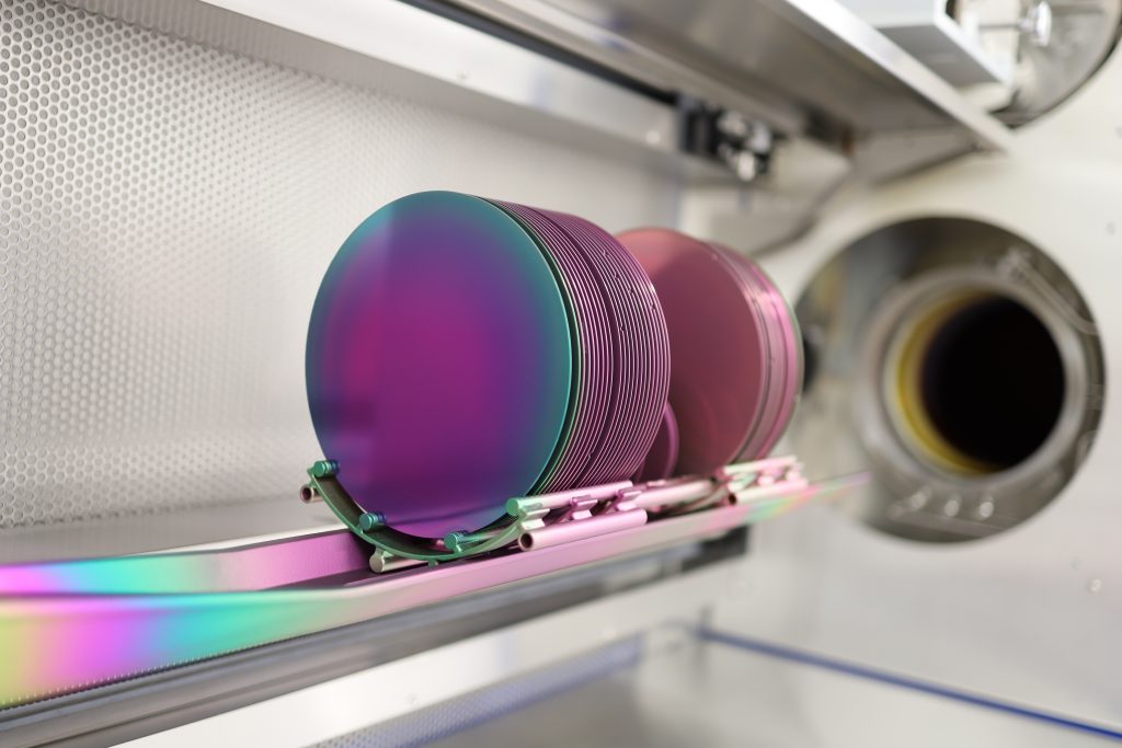
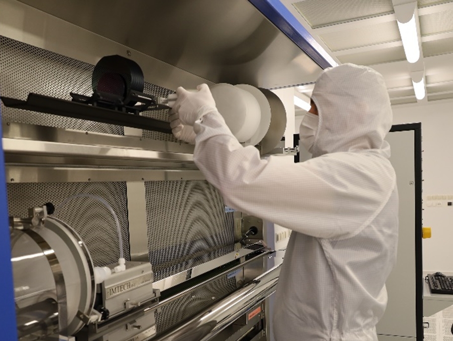
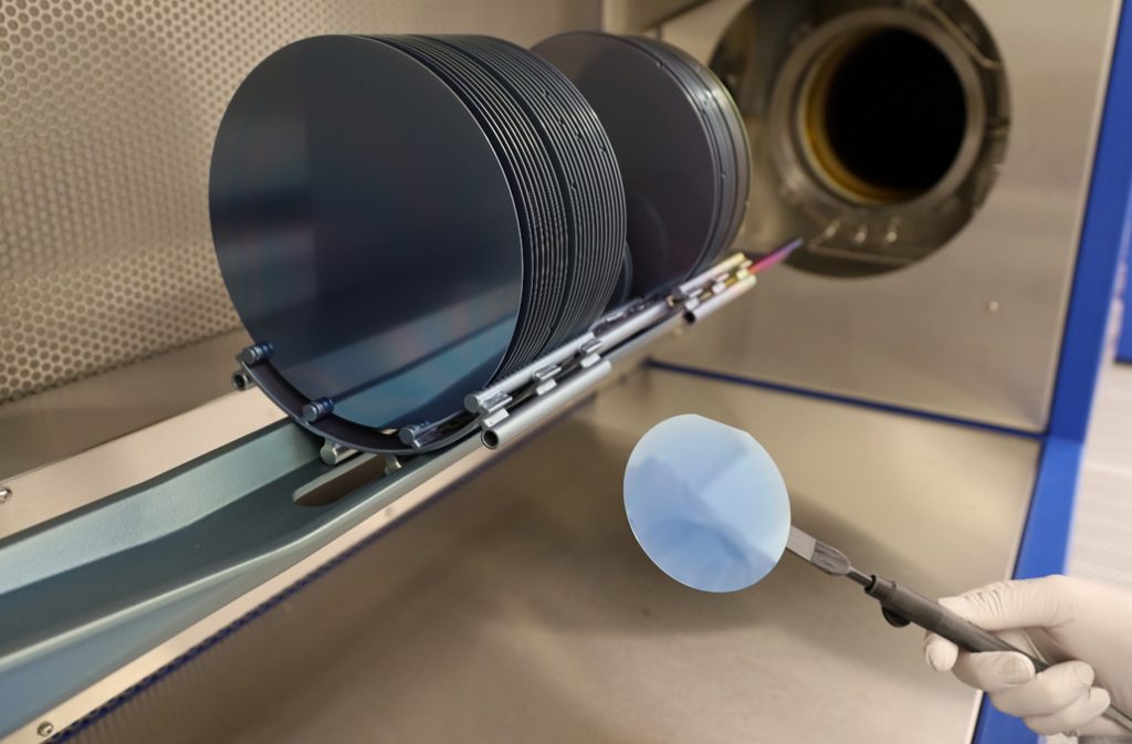
The semiconductor/planar technologies team has a state-of-the-art, high purity laboratory (ISO Class 7 to ISO Class 4) at its disposal. Research on surface preparation, thin-film fabrication, layout patterning, modification of film properties, removal/etching, and characterization is conducted in this space. Most of the work is carried out using fully automated equipment, allowing not only to obtain high repeatability of the process but also very good uniformity on silicon substrates of diameter up to 200 mm.
The described infrastructure allows for carrying out research in the field of semiconductor materials, devices and systems not only based on silicon technology but also for research on alternative materials such as gallium nitride (GaN) or silicon carbide (SiC). The team cooperates with various scientific and research units (both inside and outside the WUT).
We are open to establishing cooperation with new partners and conducting pilot and targeted work in various international and national projects. Thanks to the facilities enabling pilot or small batch production, we are also open to cooperation with industrial partners.
The team carries out work related to the modeling and technology of semiconductor devices. The conducted research concerns CMOS devices, MOS/MIM tunnel diodes, memory elements. The work also concerns the technology of nanostructures for the purposes of microelectronics and photonics. Moreover, we conduct research on semiconductor devices technology based on GaN and 2D materials (especially graphene) for the needs of THz radiation detection.