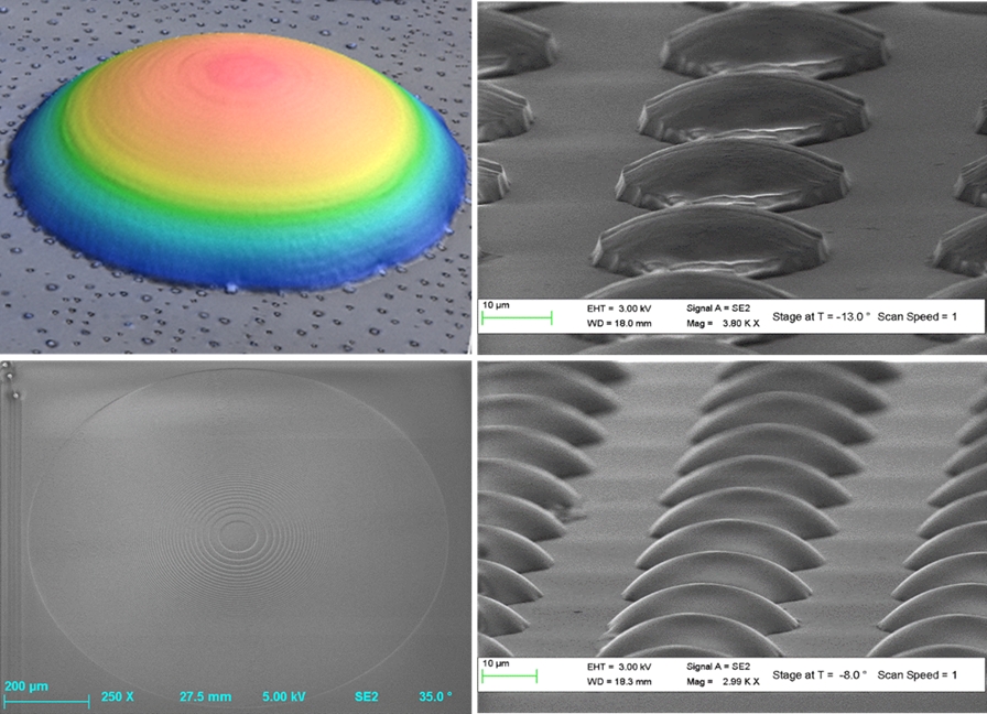
Optical Structures Technology Team designs, simulates and manufactures high precision optical elements by utilizing standard CMOS line processes. Technology is based on photolithography, electron beam lithography, layer deposition and reactive ion etching. Grayscale lithography is also available in order to manufacture features of variable height in a single process. Structures can be fabricated on flat substrates, both transparent and reflective, and on membranes as thin as 100 nm.
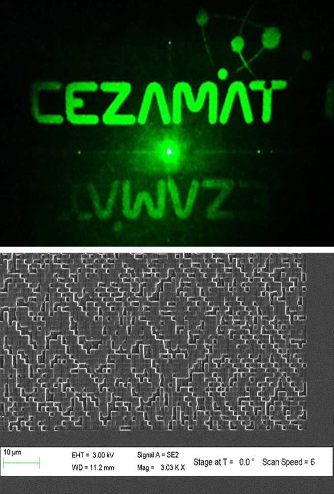
The team develops and manufactures, among others, Fresnel lenses and kinoforms with thickness between 0.5 and 3 µm and diameters up to several millimeters, reflection and transmission holograms with submicron pixel size, metastructures, diffraction gratings and microlens arrays. We have also developed manufacturing processes for extreme ultraviolet (EUV) zone plates on silicon nitride membranes, with outer ring thickness as small as 50 nm.
Fabricated elements are used in fiber coupling for photonic integrated circuits, EUV microscopy and other high precision optical systems.