The Faculty of Physics and CEZAMAT cooperate for new generation electronics
An innovative platform for the synthesis of 2D materials and their heterostructures
The Warsaw University of Technology obtained funds for the purchase of an innovative platform for the synthesis of 2D materials and their heterostructures, which will be used in nanoelectronics. The co-financing was granted by the Ministry of Education and Science as part of the investment for scientific activity.
Innovative equipment, for which the Faculty of Physics received funding in the amount of PLN 9.3 million, will enable the semi-industrial production of a wide range of two-dimensional materials, as well as their connections called heterostructures.
The system, designed in part by the department’s team of specialists in the field of structural research, will enable the growth of 2D materials intended for applications in nanoelectronics.
The new equipment will be an element of the technological hub that is being created around the Warsaw University of Technology and CEZAMAT, in which – thanks to, among others, funds from the “Science for Society” program as well as a grant from the European Commission under the EDIH program – an excellent space is created to develop cooperation with the most modern Polish technological companies.
Opportunities on a European scale
The equipment will create a research platform, unique in Europe, dedicated to the research of new two-dimensional materials and related applications. Moreover, the system may become the basis of a new technology for the future of electronics in Poland. The investment will allow for the development and deepening of current research on the world’s most modern technology for the production of materials with a two-dimensional structure.
Our researchers, who have several years of experience in working with 2D materials and producing electronic nanodevices, will ensure that the possibilities of modern equipment are fully used. The initiators of the development of this technology at Warsaw University of Technology is a team consisting of prof. Mariusz Zdrojek, prof. Włodzimierz Strupiński, Iwona Pasternak PhD and Jakub Sitek PhD.
— Our team has extensive experience in the technology of growing two-dimensional materials, which has been documented by many publications in magazines such as Nano Letters, Nanoscale, ACS Applied Materials & Interfaces and 2D Materials. Our know-how consists of patents, including the recently filed international patent for the technology of selective production of stacks of 2D materials, called heterostructures. This, combined with the team’s enormous research potential, allows us to think about a permanent remodeling of the European, and perhaps also the world stage of two-dimensional materials technology – says Jakub Sitek PhD from the Faculty of Physics of the Warsaw University of Technology. “We are already seeing the first signs of it. As part of a large European project that is being prepared, we are just starting a long-term cooperation with companies and research centers from France, Germany, Switzerland and Spain – said the researcher.
Practical applications
In recent years, world science has put more emphasis on applied applications and less on basic research. Long-term cooperation with domestic technology companies and foreign research centers is a guarantee that the results achieved thanks to the research platform will strengthen the innovativeness of the Polish economy and the reputation of Polish scientists on the international arena.
– The investment is a perfect example of seeking synergy in the joint use of both the equipment and the potential of various research teams of the Warsaw University of Technology – said Mariusz Wielec, director of the Center for Advanced Materials and Technologies CEZAMAT. The Faculty of Physics successfully engaged in another initiative of this type.
The new equipment investment may be the first step towards making Poland associated with groundbreaking achievements in the field of new 2D materials, nanoelectronics and its new varieties – including flexible electronics and twistronics, which each of us will be able to use in the future. This is an attractive prospect, especially in the context of the plans of the European Union, which wants to reactivate its independent participation in the electronics industry.
Transfer of knowledge to the economy
The benefits for the economic environment related to the purchase of new equipment are multi-level.
Industrial partners will be able to use research services, commission the production and testing of new materials, as well as the creation of special technological lines. The activities will be a continuation of the existing cooperation with Polish technological companies in the field of photonics and electronics. An example is VIGO System, which successfully uses epitaxy technology and enjoys the trust of customers from around the world.
The equipment awarded from the grant will also be used to intensify cooperation with Polish companies operating in the defense sector (WB Electronics, companies from the PGZ group).
It will also be possible to carry out joint R&D works as part of the projects of the National Center for Research and Development, the Foundation for Polish Science and own works.
Startups will also benefit – there are plans to license intellectual property in the field of the use of two-dimensional materials, and ultimately to initiate an ecosystem of new domestic startups related to the electronics industry.
World-class equipment will allow for the education of new specialists in the field of modern material technologies and stable building of staff that will develop new technologies over the coming years. This group can power a new branch of technology that is not yet available in Poland, and is the basis for the electronics of the future – Intel is considering the use of 2D materials in processors and integrated circuits, and we have a chance to provide this technology.
Persons and institutions interested in cooperation are encouraged to contact: mariusz.zdrojek@pw.edu.pl

The project Innovative platform for the synthesis of 2D materials and their heterostructures for next-generation electronics was co-financed from the state budget as part of the investment of the Ministry of Education and Science for scientific activity.
Project value: PLN 9.3 million
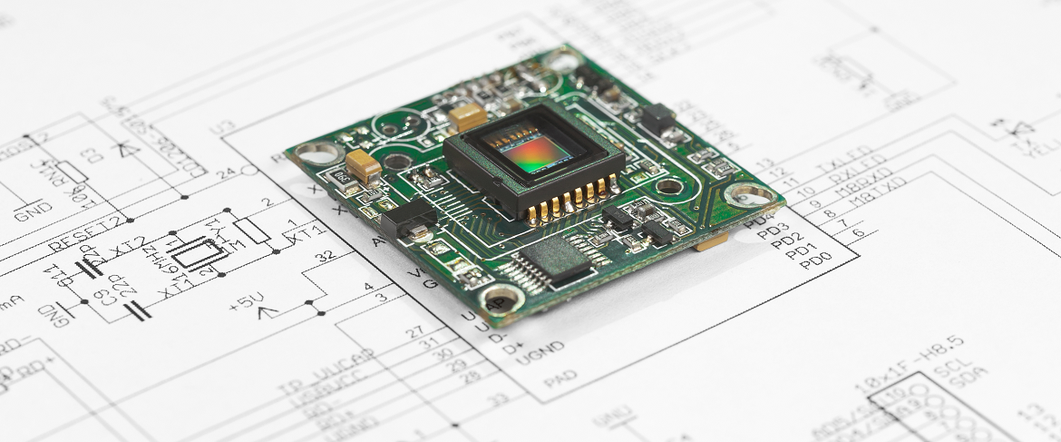
photo: iStock.com/Andrei Berezovskii